Promotional price valid on web orders only. Your contract pricing may differ. Interested in signing up for a dedicated account number?
Learn More
Learn More
Electron Microscopy Sciences Graphene on Thermal SiO2 on Ultra-Flat Silicon, 3-5 layers, 1.0-1.7 nm thick, 85.8-90.4% Transparency

Supplier: Electron Microscopy Sciences 3GUFSIO210

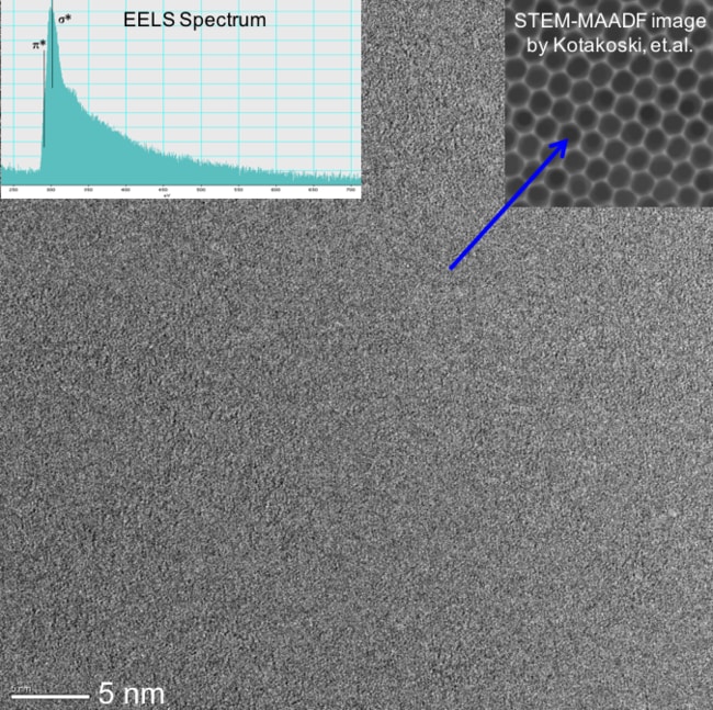
CVD graphene on ultra-flat thermal SiO2. The high quality graphene is produced by chemical vapor deposition, a process by which gaseous reactants are deposited onto a substrate. The Ultra-flat Thermal SiO2 Substrate consists of a 200 nm thermally grown SiO2 film on an ultra-flat silicon wafer with a normal thickness of 675 um. The size is 5 mm x 5 mm. Graphene coverage of the TEM grid is better than 75 percent. Available in four thicknesses of CVD graphene, 1, 2, 3-5, and 6-8.
Layers: 3-5 layers
Thickness: 1.0-1.7 nm
Transparency: 85.8-90.4%
Product Title
By clicking Submit, you acknowledge that you may be contacted by Fisher Scientific in regards to the feedback you have provided in this form. We will not share your information for any other purposes. All contact information provided shall also be maintained in accordance with our Privacy Policy.
Spot an opportunity for improvement?