
Electron Microscopy Supplies


Electron Microscopy Sciences Formvar/Carbon Film 15-20 nm/20-30 nm thick on Hexagonal 300 mesh Nickel Grid
A formvar coated grid, stabilized with evaporated carbon film. This type of coating is excellent for specimen support, especially for ultra thin sections. Coated grids are optically checked followed by batch testing in the electron microscope. Packed in grid storage box. NOTE: All film is laid on the shiny side of the grid. Formvar is 15 to 20 nm thick with a 20 to 30 nm carbon coating.
Grid: Nickel


Electron Microscopy Sciences EMS Equipment Stage 8" Stub Holder
These specimen stages are all easy-change, drop-in style (no screws), and are height adjustable. An 8" stub holder to accept up to 54 1/8 pin stubs. Compatible with EMS300TT and EMS300RD.
Electron Microscopy Sciences Athene Thick and Thin Bar Grid with Center Mark, 300 mesh Cu
Athene grids are renowned for the highest quality standards, exceptionally refined grid bars, and good handling characteristics. 3.05 mm diameter.
Grid: Copper
Electron Microscopy Sciences Quantifoil Holey Carbon Film R 5/10 on Gold 300 mesh Grid
QUANTIFOIL is a perforated support foil with pre-defined hole size, shape and arrangement. It has advantages in electron microscopy (EM) or low-energy electron point source (LEEPS) microscopy when compared with conventional holey film.
QUANTIFOIL with circular holes is used in cryo-electron tomographic reconstruction. The roundness of the holes is advantageous with respect to the formation of an ice layer of constant thickness. The whole size chosen depends on the magnification used, and on whether or not one wishes to include support film in the image. Assessment of the image quality is easier when foil is included in the picture, because the power spectrum of a foil is stronger than that of unsupported ice.
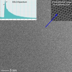
Electron Microscopy Sciences Graphene on 2000 Mesh Cu Grid, 3-5 layers, 1.0-1.7 nm thick, 85.8-90.4% Transparency
CVD graphene on microporous copper TEM grids with beryllium-copper support aperture. The graphene film appears as a near-transparent to light-grey film on the surface of the red-brown microporous copper TEM grid. For support, the TEM grid is attached using epoxy to a gold-colored beryllium-copper disk with a 2 x 1 mm aperture. Graphene coverage of the TEM grid is better than 75 percent.
Layers: 3-5 layers
Thickness: 1.0-1.7 nm
Transparency: 85.8-90.4%
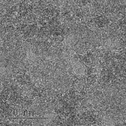
Electron Microscopy Sciences Graphene Oxide 1 Layer on Thermal SiO2 on Ultra-Flat Silicon
Graphene oxide on ultra-flat thermal SiO2.
Type: 1 layer

Electron Microscopy Sciences Lacey Carbon Film with Carbon/Formvar 1 nm / 5 nm thick on 200 mesh Gold Grid
The continuous ultrathin carbon/formvar film on lacey carbon allows for the thinnest support film that still has adequate strength to withstand electron microscope specimen preparation. The carbon 1 nm, formvar 5 nm film lies across a carbon lacey film supported by a mesh grid. The size of the holes in the lacey film differ widely from batch to batch but are generally in the range of ¼ µm to 5µm, which gives the equivalent support of at least 6000 mesh grid.
Specimen material lying over the covered holes can be imaged in the TEM with practically no interference from the carbon film supporting it. This product is ideal for looking at nanotubes, virus particles and other small particulate material.
Grid: Gold
Electron Microscopy Sciences Quantifoil Holey Carbon Film R 17/5 on Gold 400 mesh Grid
QUANTIFOIL is a perforated support foil with pre-defined hole size, shape and arrangement. It has advantages in electron microscopy (EM) or low-energy electron point source (LEEPS) microscopy when compared with conventional holey film.
QUANTIFOIL with circular holes is used in cryo-electron tomographic reconstruction. The roundness of the holes is advantageous with respect to the formation of an ice layer of constant thickness. The whole size chosen depends on the magnification used, and on whether or not one wishes to include support film in the image. Assessment of the image quality is easier when foil is included in the picture, because the power spectrum of a foil is stronger than that of unsupported ice.

Electron Microscopy Sciences EMS 200 mesh Square Grid, Copper-Rhodium
Grids are 3.05 mm diameter.
Grid: Copper-Rhodium
Thickness: Up to 27 µm, +/- 5 µm
Pitch: 125 µm
Hole: 90 µm
Bar: 35 µm
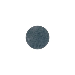
Electron Microscopy Sciences Beryllium Substrate Planchet, 50.8 mm x 1 mm
These planchets are prepared from high purity beryllium (min. 98.5%) by electro-fusion to provide vacuum tight (~1x10⁻⁹atm-cm3/sec) and +/-10% dimensional tolerances.
Size: 50.8 mm x 1 mm
Electron Microscopy Sciences Lacey Carbon Film with Ultrathin Formvar 3-4 nm thick on 400 mesh Copper Grid
The continuous ultrathin formvar film on lacey carbon allows for the thinnest support film that still has adequate strength to withstand electron microscope specimen preparation. The less than 3nm thick film lies across a carbon lacey film supported by a mesh grid. The size of the holes in the lacey film differ widely from batch to batch but are generally in the range of ¼ µm to 5µm, which gives the equivalent support of at least 6000 mesh grid.
Specimen material lying over the covered holes can be imaged in the TEM with practically no interference from the carbon film supporting it. This product is ideal for looking at nanotubes, virus particles and other small particulate material.
Grid: Copper

Electron Microscopy Sciences Formvar/Carbon Film 10 nm/20-30 nm thick on Thin Bar Square 300 mesh Gold Grid
A formvar coated grid, stabilized with evaporated carbon film. This type of coating is excellent for specimen support, especially for ultra thin sections. Coated grids are optically checked followed by batch testing in the electron microscope. Packed in grid storage box. NOTE: All film is laid on the shiny side of the grid. Formvar is approximately 10 nm thick with 20 to 30 nm of carbon.
Grid: Gold
Electron Microscopy Sciences Quantifoil Holey Carbon Film R 3/5 on Nickel 200 mesh Grid
QUANTIFOIL is a perforated support foil with pre-defined hole size, shape and arrangement. It has advantages in electron microscopy (EM) or low-energy electron point source (LEEPS) microscopy when compared with conventional holey film.
QUANTIFOIL with circular holes is used in cryo-electron tomographic reconstruction. The roundness of the holes is advantageous with respect to the formation of an ice layer of constant thickness. The whole size chosen depends on the magnification used, and on whether or not one wishes to include support film in the image. Assessment of the image quality is easier when foil is included in the picture, because the power spectrum of a foil is stronger than that of unsupported ice.
Electron Microscopy Sciences Lacey Carbon Film with Ultrathin Formvar 3-4 nm thick on 200 mesh Copper Grid
The continuous ultrathin formvar film on lacey carbon allows for the thinnest support film that still has adequate strength to withstand electron microscope specimen preparation. The less than 3nm thick film lies across a carbon lacey film supported by a mesh grid. The size of the holes in the lacey film differ widely from batch to batch but are generally in the range of ¼ µm to 5µm, which gives the equivalent support of at least 6000 mesh grid.
Specimen material lying over the covered holes can be imaged in the TEM with practically no interference from the carbon film supporting it. This product is ideal for looking at nanotubes, virus particles and other small particulate material.
Grid: Copper

Electron Microscopy Sciences Formvar/Carbon Film 25-50 nm/20-30 nm thick on Thin Bar Square 300 mesh Copper Grid
A formvar coated grid, stabilized with evaporated carbon film. This type of coating is excellent for specimen support, especially for ultra thin sections. Coated grids are optically checked followed by batch testing in the electron microscope. Packed in grid storage box. NOTE: All film is laid on the shiny side of the grid. Formvar is 25 to 50 nm thick with a 20 to 30 nm carbon coating.
Grid: Copper